
Core Competencies

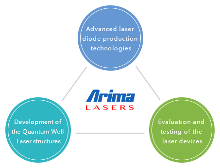
An excellent laser diode starts with the epitaxy structure design. Most of the modern high performance semiconductor lasers apply the Quantum Well structure in their epitaxy layers. That is, to uniformly grow many different thin semiconductor layers on top of the substrate like GaAs. Each layer is only several nanometers thick. By tuning the compound semiconductor materials, we can control the characteristics of the laser output.
Many things have to be considered in the Quantum Well epi structure design, such as the element composition, thickness, doping concentration, optical refraction index, chemical interaction for post processes, etc. Each of them somehow affects the final performance of the device. ALC's R&D team is specialized in the device physics and having long time experience in device structure design as well as analytical simulations. In addition to that, working closely with top research institutes enables us to establish the self-sustaining laser device technologies and leads the laser industry.
Beside the epi structure, to make a complete laser diode we need to form the micrometer range waveguides on top of the epi wafer, followed with high precision packaging. ALC applies submicron lithography, wet/dry etching, high temperature diffusion, metal evaporation, optical film coating and cleave/break processes to manufacture the optical waveguides and resonant cavities.
Top issues of the laser diode packaging are heat dissipation and alignment accuracy. Due to the high heat density in laser operation, the selection of heat sink materials and bonding conditions are greatly influential in the performance of the laser diodes. Furthermore, because laser light is directional, the bonding accuracy is highly required in order to align with customers' optical system. ALC equips with high accuracy auto packaging machines which ensure the highest quality of the laser diode manufacturing; as a result, we've gained the long time partnership with the 1st tier customers worldwide.
Due to high variety of the laser diode applications, the requirements for laser diode differ a lot. To fulfill most environmental testing conditions, ALC has set up various kinds of evaluation instruments, including the temperature/humidity controlled aging chambers, high speed pulsing testers, astigmatism tester, near field optical measurement, etc. All of these are for making sure that the devices meet all the customer requirements.
|
Production Capability
Vertical Integration
Production Control Discipline
|
||
| ALC has integrated production capability, including epitaxy growth, chip fabrication, auto precision assembly' burn-in & testing. We always quickly provide exact solution to our customers. | By strict production management and quality control, ALC keeps improving the production efficiency and yield rate. We commit to provide stable high quality products and deliver products on time. | |
|
Application Integration
Circuit Integration
Optical Integration
|
||
| Most laser applications add the feedback circuit outside of the LDs, which is used to control the laser output power stably by adjusting operating current in different temperature. This is so-called APC (Auto Power Control) circuit. ALC has developed APC ASIC integrated laser diode, which obtained multi-nation patents. This technology makes your product smaller and easier to use. Furthermore, ALC offers customized package service to customers to help increase their added values. | ALC provides customers who need specified optical output, including collimation, liner, expanding beam. Powered by our APC Laser Diode TM, we are specialized in miniaturizing laser modules with safety regulation certifications (TV). | |